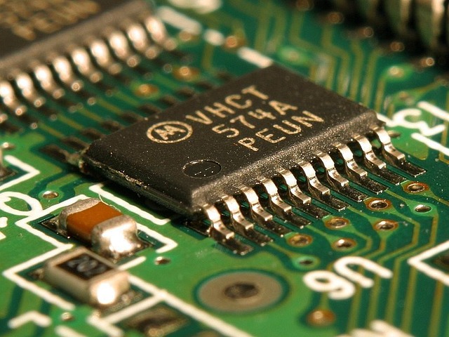
Printed Circuit Boards (PCBs) are the backbone of modern electronics. From smartphones to cars, medical devices to industrial machinery, nearly every piece of technology depends on them. Despite being a cornerstone of the electronics industry, PCB manufacturing is not free from complications. Even small errors in the design or fabrication process can lead to costly failures. Understanding the common challenges and their fixes is crucial for manufacturers, engineers, and even end-users who rely on durable and efficient boards.
In this article, we’ll explore the most frequent issues in PCB manufacturing and provide practical solutions to overcome them.
1. Design-Related Challenges
1.1 Signal Integrity Issues
Poor layout design often results in signal integrity problems, such as crosstalk, reflection, or electromagnetic interference (EMI). High-frequency signals are particularly vulnerable to these disruptions.
Fix: To resolve this, engineers should carefully design trace widths, maintain proper spacing between signals, and use ground planes for shielding. Simulation tools also help test signal flow before production, reducing the chances of layout errors.
1.2 Thermal Management Problems
Inadequate thermal planning can lead to hotspots, especially in high-power applications. Excessive heat shortens component lifespan and may cause board failure.
Fix: The solution is to integrate thermal vias, use thicker copper layers, and position components strategically to dissipate heat. Heatsinks and thermal pads may also be added for high-performance boards.
1.3 Incorrect Design Files
Sometimes, errors occur simply because of incorrect Gerber files or outdated design versions being sent to the manufacturer. These lead to misaligned layers, missing connections, or fabrication mismatches.
Fix: Always double-check design files, maintain version control, and work closely with the fabrication team. Running a Design for Manufacturability (DFM) check is a reliable way to spot mistakes early.
2. Material-Related Challenges
2.1 Substrate Quality Issues
The choice of PCB substrate significantly impacts performance. Poor-quality or inconsistent substrates may result in delamination, warping, or reduced dielectric strength.
Fix: Select materials that meet the thermal, mechanical, and electrical requirements of the final product. FR-4 is common for general applications, while high-frequency boards may need PTFE or ceramic substrates. Work with trusted suppliers to ensure consistent material quality.
2.2 Copper Thickness Variations
If the copper layer is too thin, traces cannot handle the required current. If it’s too thick, it may cause difficulties in etching or lead to uneven surfaces.
Fix: Follow IPC standards when selecting copper thickness. Manufacturers should perform routine checks to ensure uniform plating and avoid inconsistencies.
3. Fabrication Challenges
3.1 Misalignment of Layers
Multi-layer PCBs often face alignment issues during lamination. Even a slight misalignment can lead to broken connections and reduced functionality.
Fix: Precise registration systems and automated optical inspection (AOI) should be used during production. Proper temperature and pressure control during lamination also prevent shifting.
3.2 Solder Mask Defects
Problems such as misregistered solder masks, bubbles, or pinholes can expose copper traces, making them vulnerable to corrosion and shorts.
Fix: Maintaining clean production environments and calibrating printing machines regularly helps reduce defects. Automated inspection ensures solder mask accuracy before assembly.
3.3 Etching Problems
Over-etching can cause thin or broken traces, while under-etching may leave unwanted copper residues. Both affect circuit performance and reliability.
Fix: Control the etching process with proper chemical concentrations and timings. Real-time monitoring and quality control checks are essential to prevent inconsistencies.
4. Assembly Challenges
4.1 Soldering Defects
Issues such as cold solder joints, bridging, and insufficient solder are common in PCB assembly. These defects compromise electrical connections.
Fix: Optimizing solder paste application, controlling reflow oven profiles, and using automated solder inspection systems minimize soldering problems. Skilled technicians are also critical in manual soldering processes.
4.2 Component Placement Errors
Incorrectly placed or misaligned components can render a PCB useless. Human error and machine calibration issues are common causes.
Fix: Use pick-and-place machines with high precision and regularly calibrate them. Cross-verification with AOI ensures components are correctly aligned before soldering.
4.3 Tombstoning
In surface-mount devices (SMDs), small resistors or capacitors sometimes lift on one end during reflow soldering. This defect, called tombstoning, leads to open circuits.
Fix: Proper thermal balancing in pad design and optimizing reflow profiles prevent tombstoning. Equal heating of pads is crucial to maintain stability.
5. Testing and Quality Assurance Challenges
5.1 Incomplete Testing
Skipping or minimizing testing to save costs often results in defective boards reaching customers.
Fix: Every PCB should undergo functional testing, in-circuit testing (ICT), and flying probe testing when applicable. Burn-in tests are essential for boards used in critical applications such as medical or aerospace devices.
5.2 Hidden Defects
Some defects, like micro-cracks or internal delamination, are not visible during routine inspections. They only appear after the board has been in use for some time.
Fix: Employ X-ray inspection and advanced imaging techniques to detect hidden defects. Regular stress testing also identifies potential weaknesses.
6. Supply Chain and Production Challenges
6.1 Component Shortages
Global supply chain disruptions often cause delays in PCB manufacturing due to unavailability of certain components.
Fix: Maintain relationships with multiple suppliers, forecast demand early, and keep a buffer stock of essential components. Designing boards with alternate component options can also reduce dependency on specific parts.
6.2 High Production Costs
Advanced PCBs, especially those with many layers or using specialty materials, can be expensive to produce.
Fix: Cost optimization is possible through efficient design, panel utilization, and negotiation with suppliers. Outsourcing to specialized manufacturers may also reduce costs while maintaining quality.
7. Environmental and Regulatory Challenges
7.1 Waste Management
PCB manufacturing involves chemicals like etchants and plating solutions that can be harmful if not disposed of properly.
Fix: Implement eco-friendly practices, recycle materials where possible, and follow international environmental regulations such as RoHS and REACH. Investing in waste treatment systems ensures compliance and sustainability.
7.2 Meeting Global Standards
Failure to meet IPC, ISO, or CE standards can restrict a manufacturer’s ability to sell in global markets.
Fix: Stay updated with industry standards and conduct regular audits. Training staff and implementing strict quality control procedures ensure boards comply with global requirements.
8. Emerging Challenges in Modern PCB Manufacturing
8.1 Miniaturization
As electronics become smaller, PCBs must accommodate finer traces and denser layouts, which increases manufacturing complexity.
Fix: Adopt advanced fabrication techniques like HDI (High-Density Interconnect) and laser drilling for microvias. Partnering with experienced manufacturers capable of handling these designs is essential.
8.2 High-Frequency and High-Speed Boards
5G, IoT, and advanced computing applications require PCBs that can handle high-speed signals without degradation.
Fix: Use low-loss dielectric materials, maintain controlled impedance, and perform detailed signal simulations before production. These practices ensure reliable high-frequency performance.
Conclusion
PCB manufacturing is a complex process that involves multiple steps, each with its own set of challenges. From design flaws and material inconsistencies to assembly defects and supply chain disruptions, every stage requires careful attention. The good news is that most of these problems can be prevented or fixed through advanced design practices, strict quality control, and collaboration with skilled manufacturers.
By anticipating challenges and applying the right fixes, manufacturers can deliver reliable, cost-effective, and high-performance PCBs that power the technology of today and tomorrow.